Fuzz Cut is, thematically, an upgrade to Wocka, but based on a different fuzz circuit, with different (dare I say, better?) features.
There is a staggering amount of diversity in circuit design of fuzz effects over the last 60ish years. Diodes of all types, transistors, op amps, etc., etc. After poring over everything from the classic Fuzz Face, up through Devi Ever’s various designs, I finally settled on something that had a reasonable parts count and lended itself to experimentation.
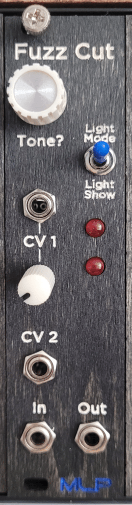
Fuzz Cut is a pretty decent fuzz on its own. It can reasonably destroy lower-harmonic waveforms (running a square wave through it is pretty pointless), with some bonus features for variety. There are two CV inputs, each affecting the voltage bias used by transistors in the circuit.
There’s a switch to select between Light Mode and Light Show. Light Mode routes the signal through the Tone? pot and has an overall less aggressive sound. Light Show bypasses the pot, which results in a hotter signal that pushes more current through the LEDs (thus giving you a light show).
Tone? has a question mark because it’s not well-labelled. The pot doesn’t really affect the tone, but I’m not sure how else to define it. It’s essentially a voltage divider that dumps some of the signal to ground, which takes some of the edge off the effect.
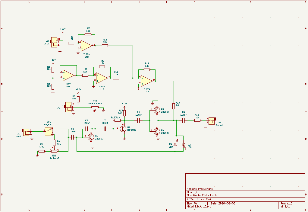
Schematic
As with any schematic found on the internet, exercise caution when building. Test the build before plugging it into your case. If you find mistakes in the schematic, or you have recommendations for improving the design, feel free to contact me and let me know.
BOM
- Capacitors
- 100nf (5) – C1, C2, C3, C4, C5
- Resistors
- 1k (2) – R15, R16
- 4.7k (1) – R1
- 10k (11) – R2, R3, R5, R6, R7, R8, R9, R10, R11, R13, R14
- 91k (1) – R4
- 3.1M (1) – R12
- Potentiometers
- 5k Tone (1) – RV1
- 100k CV Amt (1) – RV2
- Transistors
- MPSA18 (1) – Q2
- 2N2907 (3) – Q1, Q3, Q4
- ICs
- TL074 (1) – U1
- LEDs (2) – D1, D2
- SPDT Switch (1) – SW1
- Audio Jacks (2) – J1, J4
- Switched Audio Jacks (2) – J2, J3
Design Notes
There are a couple of ways you can simplify this circuit, if you want to minimize parts count (or just don’t feel like building some of the optional features).
Tone?
The input signal immediately goes through a switch, which allows for selection between Light Mode (less aggressive) and Light Show (aggressive) modes. You can pick which mode you prefer, ditch the switch and either wire the input directly C1 (Light Show mode), eliminating R1, R4 and RV1. Alternatively, you could wire the input directly to R4, ditching the switch and the path between the switch and C1.
CV 1
This control voltage implementation is relatively straightforward. We’re using an external voltage source (preferably something variable, like an LFO) to bias the collector of Q1. If you have external attenuation options, you can ditch the 100k pot. If you don’t want to use it at all, you can ditch everything except the 10k resistor to the +12V rail. At a minimum, this path to the positive power rail needs to be there.
CV 2
This CV implementation is more complex. Irritatingly so. I found the effect of the voltage sag on these transistors really interesting, but with a catch. Unlike CV 1, the voltage here couldn’t drop below a certain point, otherwise the effect stopped working.
What I’m about to tell you is unlikely to be the most elegant solution to my quandary, but it’s what I came up with, so… That’s what is in the schematic. Starting from the left, R1 and R2 create a voltage divider that reduces the power rail voltage by half. This is setting the minimum voltage for the bias–the overall bias voltage should not drop below this level, even if the CV input voltage does. This will prevent the effect from blacking out.
This minimum bias voltage needs to be combined with the CV input, so first it runs through a unity gain buffer, then through an inverting op amp (also at unity gain, just inverted).
Going back to the CV 2 input, J2 is a switched audio jack, with the tip normalled to +12V. When nothing is plugged in, it’s feeding a full 12V to the bias. Because we need to mix this with the minimum bias voltage, we’ll run it through an inverting op amp at unity gain.
Lastly, we mix the two signals by running them both through the same inverting op amp (reinverting them back to positive). The output of the op amp is limited by how close it can swing to the power rail, so even with the minimum voltage and the full +12V, the output should never exceed +12V (minus the op amp headroom). Unless, of course, I’m woefully misunderstanding how op amps work.
If all this sounds confusing and not worth the effort, you can ditch everything in this section and connect R15 directly to +12V to bias the transistors the way the Fuzz Gods intended.
Demo
Coming soon
Leave a Reply