Finally! Something that syncs. Okay, that’s in poor taste, but it really was a journey to get here. After half a dozen failed attempts to create a decent clock-syncable LFO from scratch, I decided to go in on an Electric Druid TAPLFO3 chip and put the headache behind me.
Relying largely on the datasheet, with a few tweaks, Liberty Bell 7 is an automation/modulation powerhouse: 16 waveforms, selectable unipolar/bipolar mode and a wave distortion that creates a whole spectrum of permutations on the stock waveforms.
Unfortunately, at the time of writing, US trade policy is a shitshow created by morons, and Electric Druid is not currently shipping to the US. Hopefully this gets resolved in the near future, as this chip is absolutely the bees knees.
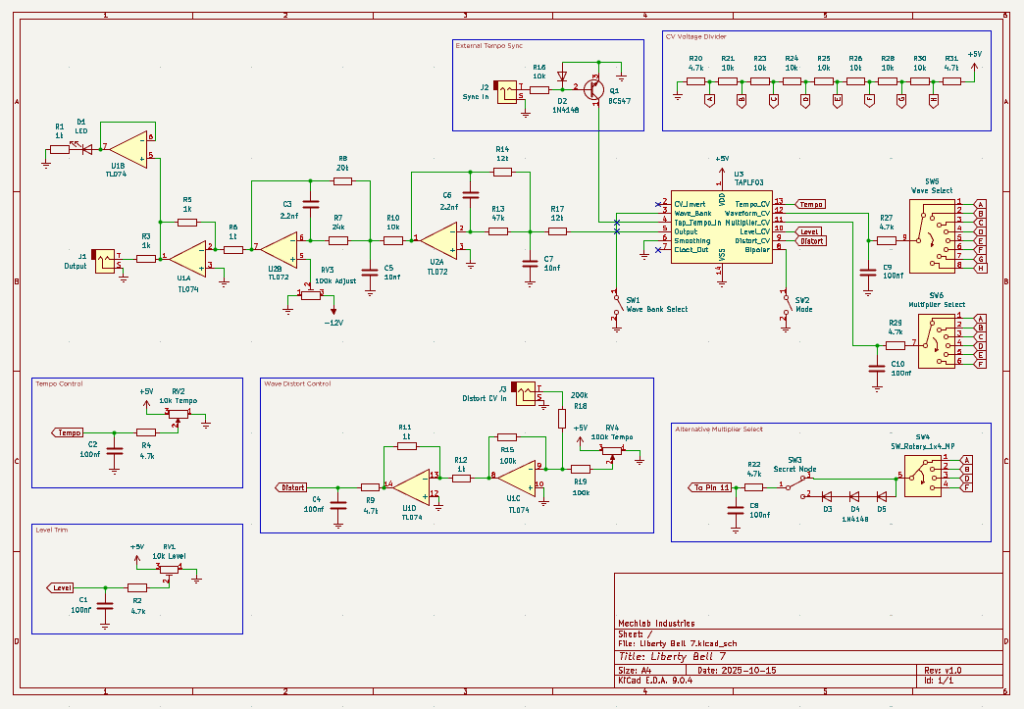
Schematic
As with any schematic found on the internet, exercise caution when building. Test the build before plugging it into your case. If you find mistakes in the schematic, or you have recommendations for improving the design, feel free to contact me and let me know.
BOM
- Capacitors
- 2.2nf (2) C3,C6
- 10nf (2) C5,C7
- 100nf (6) C1,C2,C4,C8,C9,C10
- Resistors
- 1k (6) R1,R3,R5,R6,R11,R12
- 4.7k (8) R2,R4,R9,R20,R22,R27,R29,R31
- 10k (9) R10,R16,R21,R23,R24,R25,R26,R28,R30
- 12k (2) R14,R17
- 20k (1) R8
- 24k (1) R7
- 47k (1) R13
- 100k (2) R15,R19
- 200k (1) R18
- Potentiometers
- 10k (3) RV1, RV2, RV4 (note that RV4 is labeled incorrectly in the schematic)
- 100k trimmer (1) RV3
- Transistors
- BC547 (1) Q1
- ICs
- TL072 (1) U2
- TL074 (1) U1
- TAPLFO3 (1) U3
- Diodes
- 1N4148 (4) D2,D3,D4,D5
- LEDs (1) D1
- Switches
- SPST (2) SW1, SW2
- SPDT (1) SW3*
- 8-pole rotary (1) SW5
- 6-pole rotary (1) SW6
- 4-pole rotary (1) SW4*
- Audio jacks (3) J1, J2, J3
*See frequency multiplier design notes below
Design Notes
As mentioned above, I largely stuck with the datasheet for this design, with a few notable exceptions.
CV Inputs
There’s a lot of CV control on the datasheet that didn’t seem necessary to me. So, I got rid of the CV inputs for frequency, level and waveform. By doing away with these, I could also do away with the inverting summing op amps for these controls. I kept CV input for the distort feature, because that seemed like something I’d use. But, I added an extra inverting op amp on this input, so I didn’t have to invest in the -5v power regulator and associated circuitry.
Voltage Divider
Using an analog pot to select the waveforms and frequency multiplier seemed too fraught with performance trial-and-error. I opted to implement the voltage divider array suggested in the datasheet for both features. This worked great for the waveform selecting. However, I hit a bit of a snag on the frequency multiplier.
Frequency Multiplier
There are six frequency multiplication settings, but finding a reasonably sized 6-pole rotary switch turned out to be exceedingly difficult. I had a 4-pole switch in the same form factor as the 8-pole switch I was using for the waveforms. My first thought was to ditch the 1.5x and 3x multipliers, since those are the two I’m least likely to use, but I didn’t really want to…
Necessity being the mother of invention, I opted for a combination of the 4-pole rotary switch and a SPDT toggle. The rotary switch is wired to the 0.5x, 1x, 2x and 4x multipliers. One side of the SPDT is wired directly to the rotary output (direct). The other side of the SPDT is also wired to the output of the rotary, but through three diodes in sequence (diode). The voltage drop across the diodes acts as a secondary voltage divider. With the SPDT in direct mode, the rotary switch provides 0.5x, 1x, 2x and 4x; with the SPDT in diode mode, the rotary provides 0.5x, 0.5x, 1.5x and 3x.
The schematic shows BOTH the 6-pole rotary circuit AND the 4-pole/SPDT solution. Only one of these is needed. Choose your own adventure!
Uni/Bipolar
Maybe it’s just me, but I’m finding that bipolar LFOs aren’t nearly as useful as some might think. That said, I did want to leverage the ability to switch between bipolar and unipolar modes. At first I couldn’t get the Bipolar pin to do anything. Thinking the chip might be defective, I reached out the Tom at Electric Druid. Here’s what he had to say about it:
I think this is just a misunderstanding…and that’s probably my fault for naming that pin “Bipolar”, since the output is *never* genuinely bipolar.
With the Level CV at maximum, there is no difference between the two settings of the Bipolar pin and nothing will change. If you decrease the Level CV to (say) half, you’ll start to see the difference.
What changes is the “resting level” of the waveform. In Unipolar mode, this is 0V, and increasing Level CV makes the waveform increase in a unipolar manner “from the bottom up”. In Bipolar mode, the resting level is 2.5V, and increasing Level CV makes the waveform increase in amplitude both above and below that line (hence the “bipolar” naming, although it’s not). At maximum Level CV, the waveform occupies the full range between 0V and 5V, so there’s no difference any longer.
With that cleared up, I had to rethink my approach. Fortunately, the PWM filtering stage on the output already had a zero adjust trimmer that I could use to add/remove DC offset*. That helped me with one part of the issue, for the other part…
Level Trim
According to Tom’s explanation, the Level setting plays a role in the functionality of the Bipolar pin. I have CV attenuators on most of my modules, and dedicated attenuators when I need them, so I didn’t plan to use the Level input. Per the datasheet, I had the unused pin tied to +5v through a 10k resistor. Since this sets the Level to maximum, that would render the Bipolar pin nonfunctional.
Instead, I replaced the fixed resistor to the power rail with a 10k trimmer and used that in conjunction with the zero adjust trimmer to dial in a level and offset that provided unipolar and true bipolar outputs. But that didn’t come without a trade-off…
Inverted Output
After all that, I got the pole-shifting functionality I desired, but the output was upside down. So, I added one last inverting op amp stage to flip things right-side up. Unfortunately, what I didn’t realize initially, is that this inverted the waveform and not just the voltage.
Yeah, yeah. Duh. It had been a long day.
Big deal. Where my wave should ramp up, it ramps down. Other than the graphic on the faceplate being misleading, the only real impact this has is on the waveforms the datasheet calls “Quad Ramp” and “Quad Pulse”. They’re designed to be at 0v by default, then ramp/pulse up four times in quick succession. Mine is at 5v by default, then ramps/pulses down instead. Not a deal breaker for me. I can always invert the output with an attenuverter or Voltage Daikaiju if I need it.
*Editor’s note: As I’m typing this up, it occurs to me that I could have tried skipping the Bipolar pin altogether and, instead, putting the SPST switch between the zero adjust trimmer and the negative rail. If I used the DC offset to shift the unipolar signal down to bipolar, the switch could effectively be used to turn that offset on and off. That might have been a more elegant approach that could have prevented the inverted output issues. Something to consider next time…
Demo
Coming soon
Did you build this? Let us know in the comments below!
Leave a Reply